|
Product Details:
|
| Chemical Resistance: | Yes | Processing: | Injection |
|---|---|---|---|
| Incoterms: | EXW,FOB,CIF,DDU,DDP | Property: | ESD,Non-ESD |
| Rohs Compliant: | Yes | Stacking Height: | Customized |
| Flatness: | Less Than 0.76mm | Injection Mold: | Customized Case Need (Lead Time 25~30 Days, Mold Life Span: 300,000 Times.) |
| Highlight: | Semiconductor Packaging Shippers Jedec IC Trays,ESD Jedec IC Trays,Customized Jedec IC Trays |
||
• The outline dimensions of all JEDEC matrix trays are 12.7 x 5.35 inches (322.6 x 136mm). Low profile trays with thickness of 0.25-inch (6.35mm) accommodate 90% of all standard components, such as BGA, CSP, QFP, TQFP, QFN, TSOP and SOIC. A high profile 0.40-inch (10.16mm) version is available to hold thick (high) components such as PLCC, CERQUAD, PGA (Pin Grid Arrays), modules and assemblies.
• JEDEC trays are stackable within the same device family and maker's model. Mixing multiple manufacturers' brands is not recommended, even within the same device family, due to small differences from brand to brand. While JEDEC trays may be stacked several feet high, in normal practice, stacking is limited to 5 to 7 trays.
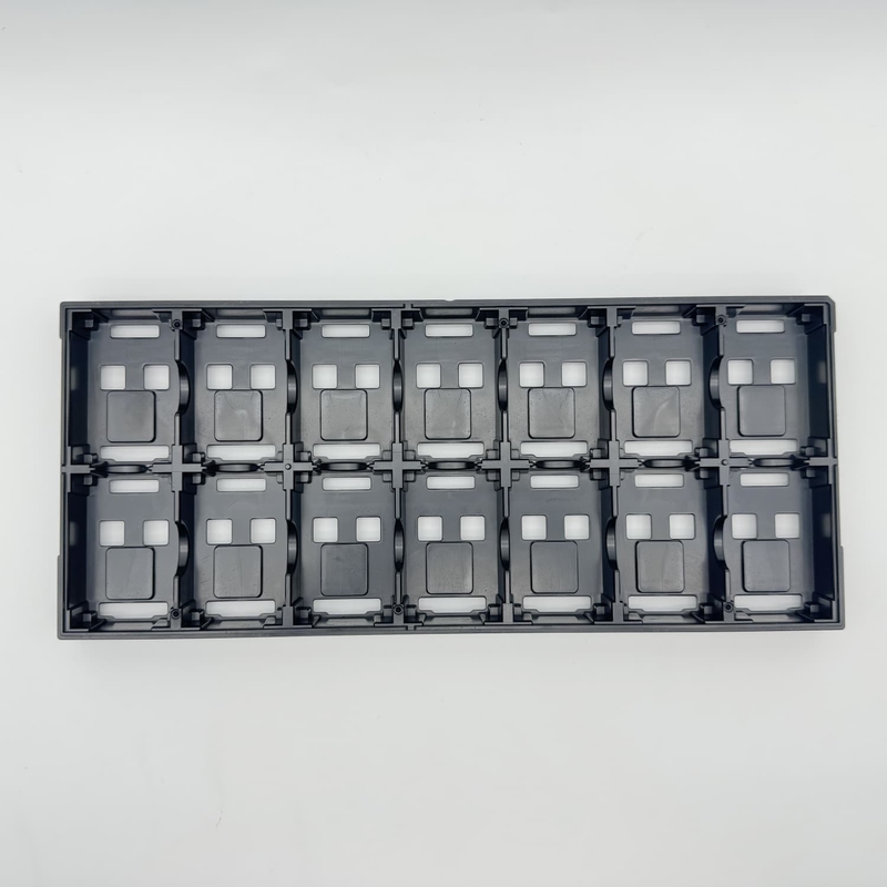
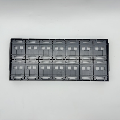
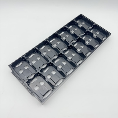
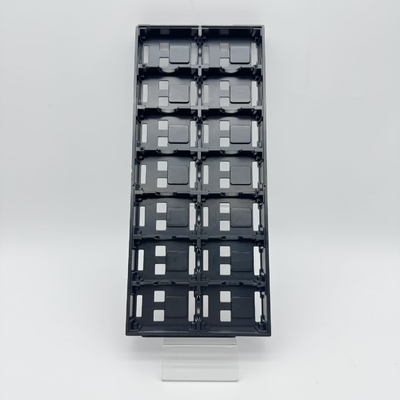
| Brand | Hiner-pack | Outline Line Size | 322.6*135.9*24mm |
| Model | HN24033 | Cavity Size | 58.4*36.83*16.62mm |
| Package Type | IC Component | Matrix QTY | 2*7=14PCS |
| Material | PPE | Flatness | MAX 0.76mm |
| Color | Black | Service | Accept OEM,ODM |
| Resistance | 1.0x10e4-1.0x10e11Ω | Certificate | ROHS |
| Usage | Packaging of Electronic Components,Optical device, |
| Feature | ESD, Durable, High Temperature, Waterproof, Recycled, Eco-friendly |
| Material | MPPO.PPE.ABS.PEI.IDP...etc |
| Color | Black.Red.Yellow.Green.White and custom color |
| Size | Customized size, rectangle,circle shape |
| Mold type | Injection Mold |
| Design | Original sample or we can create the designs |
| Packing | By Carton |
| Sample | Sample time: after draft confirmed and payment arranged |
| Sample charge: 1. Free for stock samples | |
| 2. Custom Tray negotiated | |
| Lead Time | 5-7 Working days |
| The exact time should according to the ordered quantity |
• When JEDEC developed its matrix tray standard outline, all focus was placed on the external size and features. The interior was intentionally left undefined and unrestricted. This left the door open for the matrix tray outline to be used for an unlimited variety of products and components.
• The first JEDEC Trays were designed for the semiconductor industry. These trays are often referred to as IC matrix trays. This continues to be the most common use with trays used for through-hole devices like PGA, DIP, and TO packages; surface mount devices like, QFP, BGA, TSOP, and FP packages; and leadless devices like LGA, QFN, and LCC packages.
• Today, other electronic components like connectors, sockets, adapters, PCBs, MEMS, and a wide range of small assemblies are handled in JEDEC matrix trays to facilitate assembly and pick-and-place processing. Non-electronic components, including lenses, watch parts, formed metal pieces, even synthetic stones, are processed in JEDEC outline matrix trays so that standardized automation equipment can be used.
Contact Person: Rainbow Zhu
Tel: 86 15712074114
Fax: 86-0755-29960455