|
Product Details:
|
| Compatibility: | JEDEC Standard | Anti-Static: | Yes |
|---|---|---|---|
| Custom: | Support | Pocket Size: | 9.3x9.3x2.22mm |
| Use: | Transport,Storage,Packing | Color: | Usual Black |
| Material: | MPPO.PPE.ABS.PEI.IDP | Hs Code: | 39239000 |
| Highlight: | JEDEC trays supplier,Anti-Static Jedec IC Tray,CQFP48 Package Chips JEDEC trays |
||
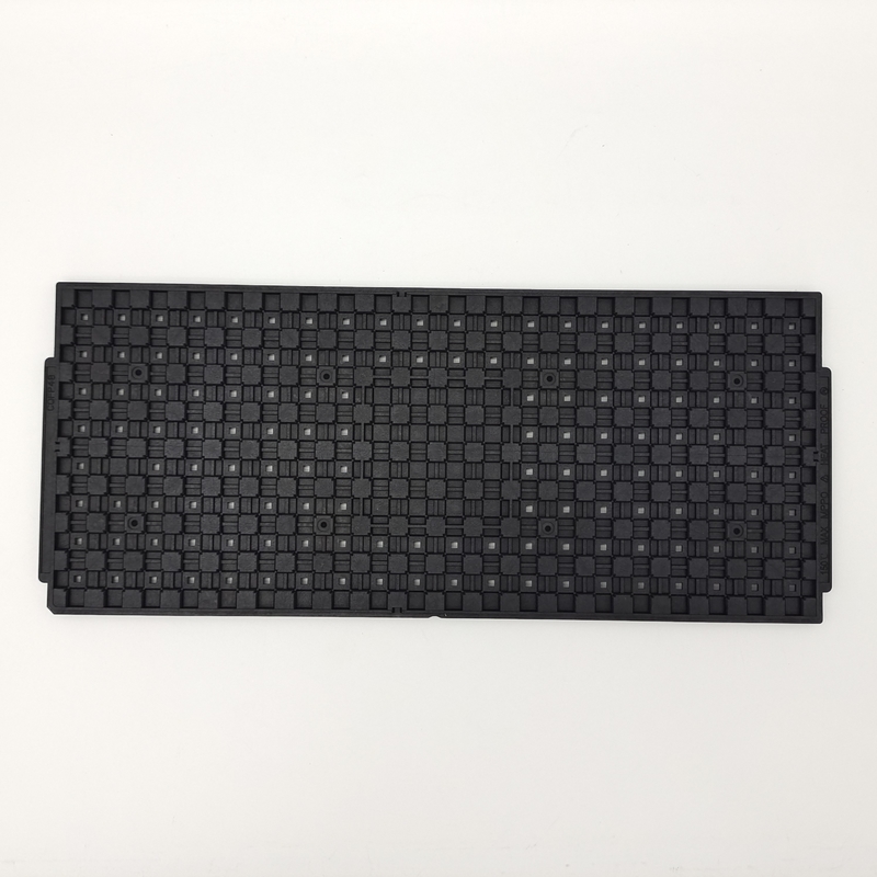
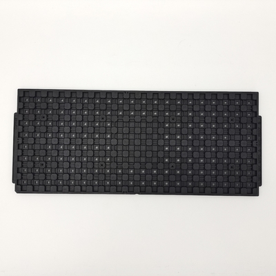
JEEDC IC Tray For CQFP48 Package Chips Meets Environmental And Rohs Requirements
Hiner-pack was founded in 2013,it is a high-tech enterprise which is integrated Design,R&D,Manufacturing,Sales of IC packaging and testing as well as semiconductive wafer fabrication process in automated handling,carrying,transportation to provide customers turnkey services.
Customized cases : 5G Core Part, Socket, RF Chip, MEMS, Optical Chip
The JEDEC trays have been specifically designed and manufactured to fit seamlessly with standard handling and testing equipment. They are readily compatible with pick-and-place machines which greatly streamlines the manufacturing process.
While there are standard designs available for JEDEC trays, some manufacturers offer additional customization to accommodate specific device shapes or sizes. This provides flexibility in the manufacturing process and ensures that the trays can be tailored to meet individual requirements.
| Customized Size | |
| Item Material | ABS / PC / MPPO / PPE... acceptable |
| OEM&ODM | YES |
| Item Color | Can be customized |
| Feature | Durable;Reusable;Rcofriendly;Biodegradable |
| Sample | A. The free samples: choosen from existing products. |
| B. customized samples as per your design/demand | |
| MOQ | 500pcs. |
| Packing | Carton or as per customer's request |
| Delivery time | Usually 8-10 working days,depends on order quantity |
| Term of payment | Products:100% prepayment. Mold:50% T/T deposit, 50% balance after sample confirmation |
![]()
At Hiner-pack, our customized JEDEC TRAY is designed to 100% meet your IC's specifics, providing tailored protection solutions based on its chip packaging. Our website showcases our range of JEDEC TRAY designs for multiple packaging type, including but not limited to BGA, FBGA, LGAQFN, QFP, PGA, TQFP, LQFP, SoC, and others. We can deliver effective design solutions and effective wafer-level package protection for your products.
Hiner-pack specializes in Research & Application for semiconductor packaging and modified material,which industry chain has integrated the raw materials,mold,the finished product and dust free clean.Our engineering technicians can offer from the mold design,material evaluation,the finished product to the dust free clean in one-stop to provide a full range of solutions,that can effectively save the cost for customers.Our company has skillful and well-trained team in the field of Semiconductor packaging design to work out customer’s requirements,for instance,different temperature,color,ESD property and cleanliness class etc.Experienced product structure engineering team can design various of IC chip,wafer,precision components packaging methods and specifications and other special demands to fit you well.
| HN PN. | Description | External Size/mm | Pocket Size/mm | Matrix QTY |
| HN23123 | CQFP48 | 322.6x135.9x7.62 | 9.3x9.3x2.22 | 8X20=160PCS |
| TYPE | Brand | Flatness | Resistance | Service |
| BGA IC | Hiner-pack | MAX 0.76mm | 1.0x10e4-1.0x10e11Ω | Accept OEM,ODM |
![]()
Product Packaging:
Contact Person: Rainbow Zhu
Tel: 86 15712074114
Fax: 86-0755-29960455